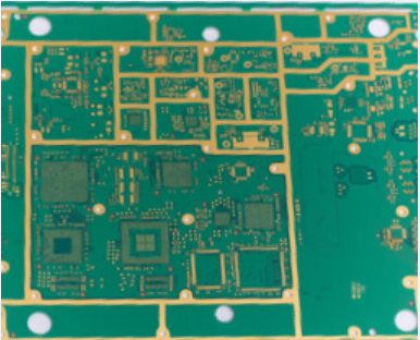
High Density Interconnect PCBs
High-Density Interconnect (HDI) is simply a PCB with more number of interconnections, occupying minimal space. This results in the miniaturization of the circuit board. The components are placed closer and the board space is significantly reduced but the functionality isn’t compromised. To be more precise, a PCB with an average of 120 to 160 pins per square inch is considered as an HDI PCB. The HDI design incorporates dense component placement and versatile routing. The HDI popularized microvia technology. A denser circuitry is crafted with the implementation of microvias, buried vias, and blind vias. The drill to copper is reduced in an HDI design.
Key Features and Benefits
- Phenomenal versatility
- Compact design
- Better signal integrity
- High reliability
- Cost-effective
- Smaller, lighter boards with more functionality
- Laser direct drilling
- Implementation of Blind, buried, and microvias


